|
1. Metamaterials for application in STEALTH technology |
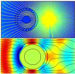
Fig. 1. Full (a) and partial (b) cloaking of an object by utilizing a meta- material with specifically designed permittivity and/or permeability |
Creating artificial materials with pre-set optical properties is of enormous importance for a variety of civil and military applications. In 2006 Pendry[1], and co-workers proposed electromagnetic (EM) cloaking of an object in the GHz range. To achieve this phenomenon, the object is encapsulated by shell made of a metamaterial with specifically designed permittivity and permeability (see Fig. 1). When both the permeability and permittivity are negative a rather peculiar phenomenon referred to as negative refraction is observed. In such media many optical processes are reversed, including Snells law, Doppler effect, etc. Recently, we have demonstrated such bulk metamaterials in the optical range [2]. Despite the progress, however, it is important to design new non-resonant and thus low loss metamaterials that could provide a high level of electromagnetic invisibility at the macroscopic scale. A theoretical study of such materials is the main emphasis of our current efforts. [1] J. B. Pendry, et. al., Controlling Electromagnetic Fields, Science 312, pp. 1780 (2006). [2] J. Valentine, S. Zhang, T. Zentgraf, E. Ulin-Avila, D. A. Genov, G. Bartal and X. Zhang, Three Dimensional Optical Metamaterials Exhibiting Negative Refractive Index, Nature, Vol. 455, pp. 376 (2008). [3] S. Zhang, D. A. Genov, and X. Zhang, Matter wave cloaking, Physical Review Letters, vol. 100, pp. 123002 (2008). |
|
2. Exotic optical applications The recent explosive development of the area of metamaterials opens the possibility to manipulate light at will. This is accomplished by precise engineering of the microscopic magnetic and electric response of the media and is equivalent to virtually creating new types of quasi-atoms and quasi-molecules. As a result unbounded possibilities arise for making novel optical devices and theoretically studies of the fundamental properties of light interaction with matter. Two particular examples of those capabilities are discussed below. |
|
A) Photonic traps: In a recent work[4], we have shown that the metamaterial concept can be utilized to precisely canal the electromagnetic flow in any possible direction, resulting in extremely high energy densities. Furthermore a specially engineered composite media can serve to mimic the photon motion around massive gravitational objects such as black holes in controlled laboratory environment. Possible applications of the proposed novel media in the form of continuous index photon traps (CIPT) are the subject of our current efforts. |
|
|
| [4] D. A. Genov, S. Zhang, and X. Zhang, Mimicking celestial mechanics in metamaterials, Nature Physics 5 (9), 687 (2009). |
| Fig. 2. Light interaction with a photonic black hole made of a composite metamaterial. Incident of Gaussian beams with wavelenghts 0.5µm (a), 1µm, (b), and plane wave with wavelenght 0.5µm (c), results into critical behavior with part of the energy collapsing at the center singularity while the rest is scattered in the far-field. |
|
B) Extreme sub-wavelength light manipulation and imaging: The major challenge in scaling-down integrated photonics is how to overcome the diffraction-limit. A high index solid immersion lens can improve the spatial resolution of a microscope by increasing the medium refractive index, but only to few times higher than in air. Photonic crystals can guide light in three dimensions; however, the guided beam width is at most a half wavelength in size. Surface plasmons have a potential to reach the sub-wavelength scales; nevertheless, they are confined at two-dimensional. In this project we study new types of optical materials that map conformal spaces and may allow molding the light flow at the deep sub-wavelength scale in all three dimensions(see Fig. 3). These novel materials can be use for optical imaging and lithography with resolution far surpassing the current state of art. [5] S. Han, Yi Xiong, D. Genov, Z. Liu, G. Bartal and X. Zhang, "Ray Optics at a Deep-Subwavelength Scale: A Transformation Optics Approach", Nano Letters 8, 4243 (2008). |
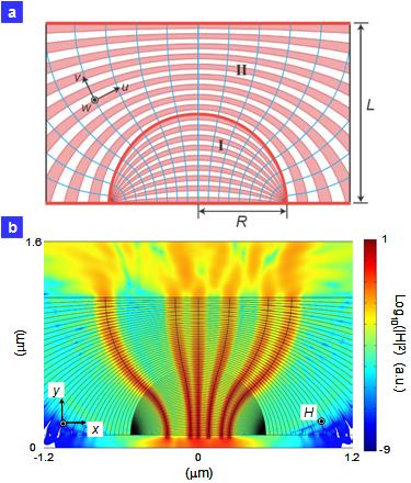
Fig. 3. Finite Difference Frequency Domain (FDFD) simulation of beam guiding with beam size only 1/10 |
|
3. Nanoscopic light emitters and nanolaser systems |
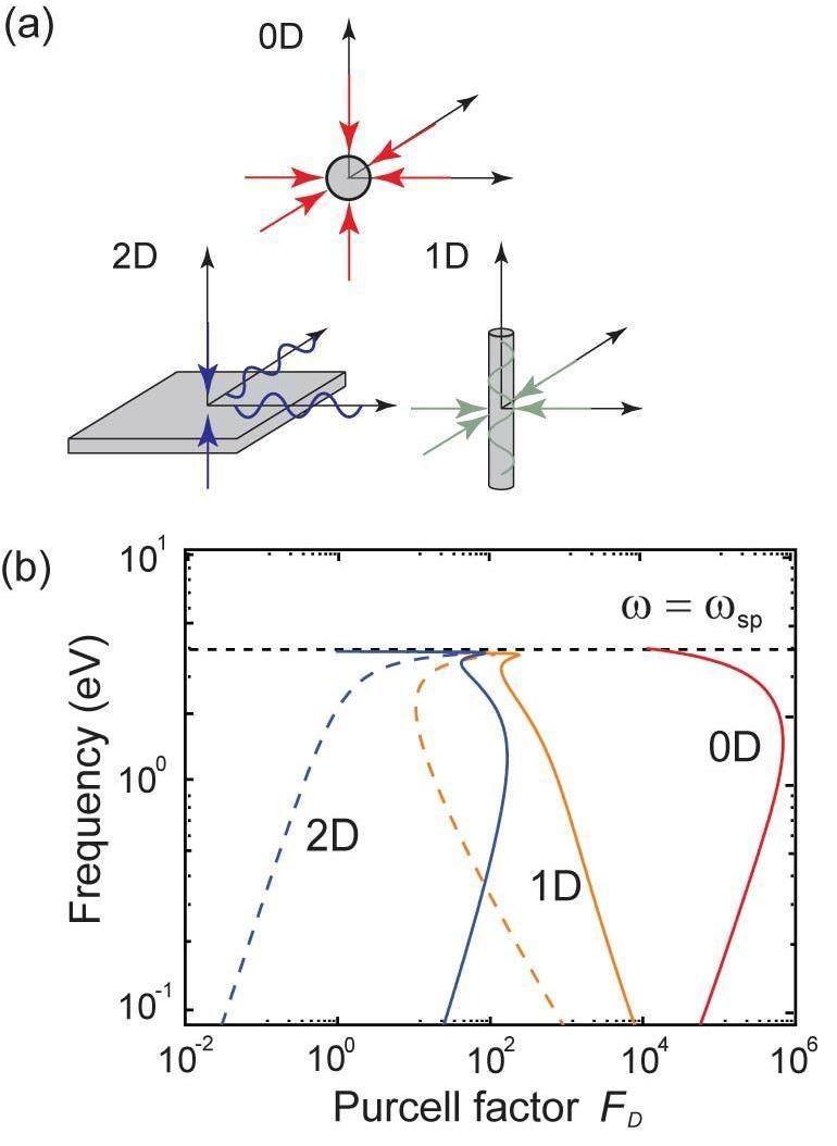
Fig. 4. (a) Metal nanosctructures supporting SP modes with varying optical degrees of freedom (ODF) can provide dramatic spontaneous emission rate enhancement (b) for emitters coupled to SPs. The 0D case sets the limits of plasmonics. |
Compared with the wavelength of light, the length scale of an exciton recombination event is typically less than the excitons Bohr radius; this leads to a broad angular spectrum of evanescent waves at visible frequencies that can not couple to the far field. However, reducing the sizes of optical modes to match those of an emitter opens a channel to these untapped evanescent waves. Such canals can be readily provided by surface plasmons states that are characterized by greatly reduced mode sizes (see Fig. 4). Additionally, introduction of an active media could substantially decrease intrinsic losses in metals; thus overcoming many limitations of a wide range of optical devices[6]. For instance, the intrinsic losses put an absolute limit on the surface plasmon propagation length at a metal interface, and set the maximum local field enhancement in random metal composites. This project will study the potential for decrease of dissipation resulting in highly efficient plasmon waveguides with modes sizes much smaller than free space wavelength, development of extraordinary sensitive SERS substrates for bio-sensing and spectroscopy, and implementation of plasmonic superlen with unsurpassed spatial resolution. Furthermore, coupling of dipole radiation into SP modes with various degrees of freedom (see Fig. 4) can provide new applications such as fast optical switching and laser operation with bandwidths surpassing 1THz. [6] D. A. Genov, M. Ambati, and X. Zhang, Surface Plasmon Polariton Amplification in Planar Metal Films, IEEE Journal of Quantum Electronics, vol. 43, No.11, pp. 1140 (2007). |
|
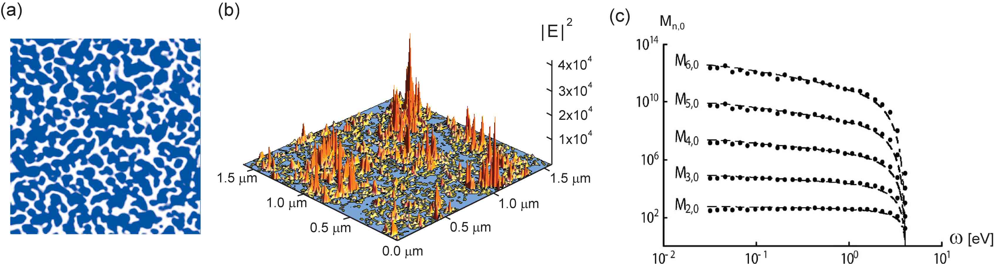
4. Electromagnetic properties of complex media Nano-structured random composite materials exhibit anomalous phenomena such as extraordinary enhancements of linear and non-linear optical processes due to excitation of collective electronic states, surface plasmons (SP) (see. Fig. 5). Under illumination with light the SP act as nanoscopic energy concentrators undergoing intricate geometrical phase transition at critical metal concentrations[7,8]. The unique properties of the percolating films make them ideal not only for fundamental studies of light interaction in random systems, but also for a wide range of applications in bio-sensing, spectroscopy, material science, and optics. That is why it is important to develop novel numerical methods for calculating the electromagnetic (EM) respons of large 2D and 3D systems of particles. Seeking new highly efficient numerical algorithms and utilization of the Louisiana Optical Network Initiative (LONI) supercomputing facilities for fast parallel calculations is the main subject of this project. |
|
|
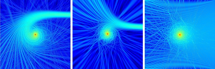
Fig. 5. Inhomogeneous metal films (a) are composed of nanometerin size metal particles deposited on a dielectric surface. Illumination of the film with an EM wave (E0 =1) results in giant local field intensity fluctuations. The enhanced fields correspond to excitation of localized surface plasmon modes. At critical metal concentrations, the random films are inhomogeneous and self-similar (fractal) in nature. Thus, for any incident wavelength resonating clusters exist in the composite; (b) 0.4µm, (c) and 1.5µm. |
|
[7] D. A. Genov, K. Seal, X. Zhang, V. M. Shalaev, A. K. Sarychev, Z. C. Ying and H. Cao, Collective Electronic States in Inhomogeneous Media at Critical and Subcritical Metal Concentrations, Physical Review B - Rapid Communications, vol. 75, pp. 201403(R), (2007). [8] D. A. Genov, A. K. Sarychev and V. M. Shalaev, Surface plasmon excitation and correlation-induced localization-delocalization transition in semicontinuous metal films, Physical Review B Brief Report, vol. 72, pp. 113102 (2005). |