Dr. Arden L.Moore
The Multiscale Energy Transport and Materials Laboratory at Louisiana Tech University
Research
Current research areas include:
- Micro/nanoscale physics of phase change heat transfer
- Nanostructure-enhanced phase change heat transfer
- Thermal transport in nanostructures (diamond nanoparticle thin films, h-BN thin films, nanowire networks, etc.)
- Materials and techniques for advanced thermal management of electronics
- Novel Monte Carlo approaches to the modeling of nanoscale coupled electrothermal transport
- Optical, thermal, chemical, and environmental sensing
- Advanced manufacturing techniques (selective laser melting, additive manufacturing, etc.)
- Methods and materials for high efficiency energy conversion
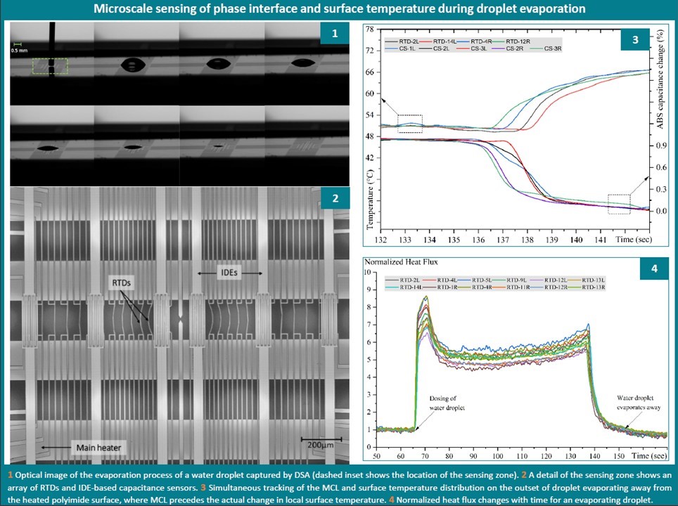
Independent microscale sensing of phase interface and surface temperature during droplet evaporation Despite the important and pervasive nature of evaporative heat transfer phenomena, fundamental questions still remain about the microscopic processes that occur in and around individual droplets on a surface. In order to understand the underlying physics behind evaporative heat transfer, it is critical to have information at the individual droplet level regarding the surface temperature distribution with time as well as the location and speed of the moving multiphase contact line (MCL). In this work, a multifunctional microscale device comprised of a resistance heater, an array of spatially distributed thin-film resistance temperature detectors, and a phase interface sensing capacitance micro-sensor array has been utilized to measure the local heat transfer characteristics and MCL behavior simultaneously for the evaporation of individual sessile water droplets on a horizontal heated surface. The resistance- and capacitance-based operating principles of the micro-device means that it is capable of detecting temperature changes and tracking MCL at the microscale in real time even for applications with limited or no visibility such as within thermal management hardware or processing equipment. Importantly, having knowledge of the MCL’s location and speed with microscale precision allows for its influence on surface temperature and heat transfer to be directly studied rather than inferred. Results show that the MCL passage precedes the change in local surface temperature and the duration of the time difference between these events depends on the MCL’s speed. In addition, the passage of the MCL accounts for more than 70% of the overall temperature change during the evaporation process.. Mondal, M. T. H., Hossain, R.,, Martin, R., and Moore, A. L., “Independent microscale sensing of phase interface and surface temperature during droplet evaporation” Applied Thermal Engineering 236, 2024, 121447. DOI: 10.1016/j.applthermaleng.2023.121477 [Link]
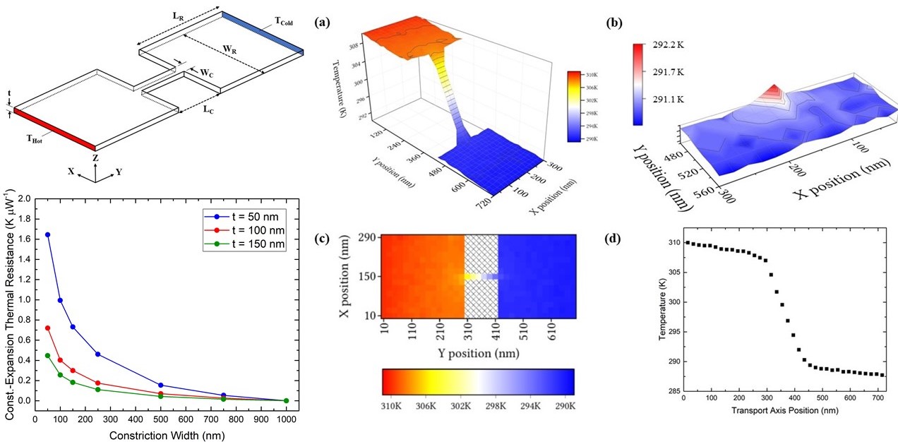
Phonon thermal transport in silicon thin films with nanoscale constrictions and expansions In patterned thin film devices, abrupt geometric changes can introduce thermal constriction and expansion resistances whose magnitude and relative importance depends on the device’s size and geometry as well as the dominant heat carrier mean free path spectra of the comprising material. Existing analytical models of thermal constriction and expansion resistances at the nanoscale have focused primarily on semi-infinite geometries or other situations which are quite different from those encountered in modern nanopatterned thin film devices. In this work, Monte Carlo methods are used to simulate phonon transport in silicon thin films patterned with a commonly utilized source-channel-drain geometry. The length, width, and thickness of the channel region were varied and the dependence of the thermal constriction-expansion resistance on these parameters was determined. Results show that thin film source-drain reservoirs with diffuse boundary scattering do not behave as semi-infinite reservoirs for feature sizes smaller than approximately 100 nm in silicon near 300 K, and that existing analytical models cannot be readily applied to such systems. In addition, our results support the case that ballistic phonon effects in silicon nanowires at room temperature, if present, are small and not easily observable. Finally, we provide guidance and perspective for Si nanowire measurements near room temperature as to what scenarios may lead to a non-negligible amount of error if constriction-expansion geometry effects are ignored. Spence, T. J. and Moore, A. L., “Phonon thermal transport in silicon thin films with nanoscale constrictions and expansions ” Journal of Applied Physics 131, 2022, 025106. DOI: 10.1063/5.0063744 [Link]
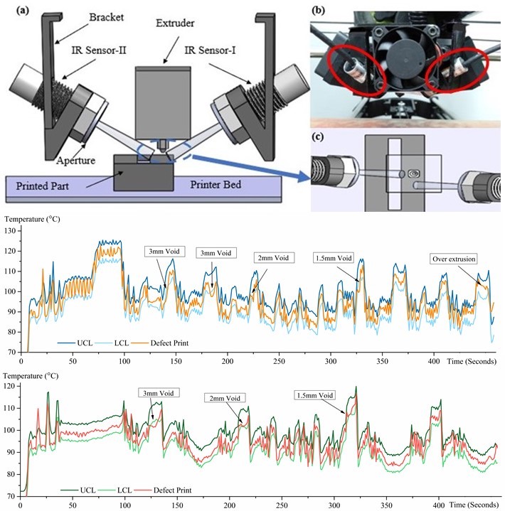
In situ infrared temperature sensing for real-time defect detection in additive manufacturing Melt pool temperature is a critical parameter for the majority of additive manufacturing processes. Monitoring of the melt pool temperature can facilitate the real-time detection of various printing defects such as voids, over-extrusion, filament breakage, clogged nozzle, etc. that occur either naturally or as the result of malicious hacking activity. This study uses an in situ, multi-sensor approach for monitoring melt pool temperature in which non-contact infrared temperature sensors with customized field of view move along with the extruder of a fused deposition modeling-based printer and sense melt pool temperature from a very short working distance regardless of its X-Y translational movements. A statistical method for defect detection is developed and utilized to identify temperature deviations caused by intentionally implemented defects. Effective detection for multiple defect types and sizes is demonstrated using both a simple L-shaped test geometry and a more complex industry standard test article. Strengths and limitations of this approach are presented, and the potential for expansion via more advanced data analysis techniques such as machine learning are discussed. Hossain, R., Lewis, J., and Moore, A. L., “In situ infrared temperature sensing for real-time defect detection in additive manufacturing ” Additive Manufacturing 47, 2021, 102328. DOI: 10.1016/j.addma.2021.102328 [Link]
![]()
Microscale tracking of unconstrained moving multiphase contact lines via a capacitance sensor array The ability to track the spatial location of a moving multiphase contact line in time significantly enhances understanding into the fundamental physics behind biological processes, condensation- and evaporation-based heat transfer, and a host of other important phenomena. In this work, we present a capacitance-based microdevice capable of tracking a moving phase interface at the microscale for an unconstrained liquid droplet. The microdevice is comprised of an array of planar interdigitated electrodes beneath a thin insulating polymer layer. Monitoring changes in capacitance with time facilitates sensing of the multiphase contact line location and speed as it passes over each capacitance sensor in turn. This capacitive sensing scheme is designed to be highly sensitive and noninvasive to the droplet under study. Results show the speed and location of moving multiphase contact lines for advancing and receding water droplets are indeed able to be detected through the change in capacitance signals in the sensor array. It is also shown that the array can be used to measure the advancing and receding contact angles of unconstrained droplets. Mondal, M. T. H., Desai, T., Hossain, R., and Moore, A. L., “Micro-scale tracking of unconstrained moving multiphase contact lines via a capacitance sensor array ” Sensors and Actuators A: Physical 331, 2021, 113046. DOI: 10.1016/j.sna.2021.113046 [Link]

Spatially Periodic Vapor Bubble Activity During Subcooled Pool Boiling on 1D Aluminum Alloy Micro-Fin Arrays Within the broad field of micro- and nano- scale surface modification to improve pool boiling performance, micro-fin arrays are especially attractive due to their ability to significantly increase wetted surface area with minimal increase in size or weight compared to macroscopic fins. In addition, their regular and repeating geometry enables greater potential for parametric optimization, uniformity, and repeatability as compared to more randomized alternatives. However, the presence of a regular, repeating microscale pattern on a heated surface has previously been shown to create alternating regions of liquid and vapor flow at small length scales which can strongly affect the macroscopic heat transfer performance of the surface. In this work, a combination of pool boiling experiments, high-speed imaging, and numerical modeling were used to investigate vapor bubble behavior and pool boiling heat transfer characteristics from one-dimensional (1D) aluminum alloy micro-fin arrays in the dielectric coolant HFE-7100. Results showed that the presence of 1D micro-fin arrays can significantly enhance pool boiling performance above that of a planar, unpatterned baseline surface but with important and sometimes nonintuitive dependence on micro-fin height. Experimental data indicated that a simple increase in surface area does not necessarily correlate to improved heat transfer performance, while high-speed imaging revealed that the presence of the micro-fins induces a periodic series of upward and downward flow patterns, in addition to distinct vapor bubble migration behavior. These results expand the range of surface types and working fluids for which spatially periodic and distinct liquid/vapor transport pathways created via microscale surface modification have been reported. Doran, B., Zhang, B., Davani, S., Osafo, K. A., Sutka, O., Walker, A., Mueller, N., Akwaboa, S., Mensah, P., Meng, W. J., and Moore, A. L., “Spatially periodic vapor bubble activity during subcooled pool boiling on 1D aluminum alloy micro-fin arrays,” International Journal of Heat and Mass Transfer 180, 2021, 121760. DOI: 10.1016/j.ijheatmasstransfer.2021.121760150585. [Link]

Experimental determination of the role of increased surface area in pool boiling from nanostructured surfaces (Top, left) Top-down SEM image of a nanoporous anodic aluminum oxide (AAO) coating which provides significantly increased surface area without an increae in microscopic nucleation site density or enhanced wicking action. (Top, right) Image of nucleate boiling from an AAO sample under test. (Bottom, left) Subcooled pool boiling performance comparison between three AAO samples and three samples with a solid native alumina oxide thin flim coating. (Bottom, right) Results of analytical modeling which shows that the nanopores are too small to act as individual nucleation sites. Doran, B., Zhang, B., Walker, A., KC, P., Meng, W. J., and Moore, A. L., “Experimental determination of the role of increased surface area in pool boiling from nanostructured surfaces,” Experimental Thermal and Fluid Science 111, 2020, 109956. DOI: 10.1016/j.expthermflusci.2019.109956 [Link]
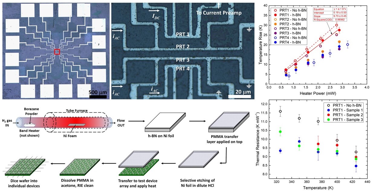
APCVD hexagonal boron nitride thin films for passive near-junction thermal management of electronics (Top, left) Annotated optical microscope images of a representative sample. (Left) An individual microdevice with transferred h-BN thin film. Large square features around the periphery are contact pads. The central test region with four-probe PRTs is outlined in red. (Right) Detail of the red-boxed region showing the h-BN thin film entirely overlaying the four four-probe PRT lines. Annotations indicate application of DC heating (IDC) and smaller AC sensing (iac) currents. Inner electrodes without annotation were used for measuring the voltage drops in the four-probe regions of each PRT using either a voltage preamplifier in the case of PRT1 or a lock-in amplifier in the case of PRTs 2-4.(Bottom, left) APCVD growth and PMMA-assisted transfer process flow for realizing h-BN thin films on prefabricated microdevice arrays. (Top, Right) Steady-state temperature rise of PRT1 (heater), PRT2, PRT3, and PRT4 for Sample 2 (filled symbols) and the blank microdevice (open symbols) at a temperature of 375 K. (Bottom, Right) PRT1 effective thermal resistance for all four measured devices versus stage temperature. KC, P., Rai, A., Ashton, T. S., and Moore, A. L., “APCVD Hexagonal Boron Nitride Thin Films for Passive Near-junction Thermal Management of Electronics,” Nanotechnology 28(50), 2017, 505705. DOI: 10.1088/1361-6528/aa97ae [Link]
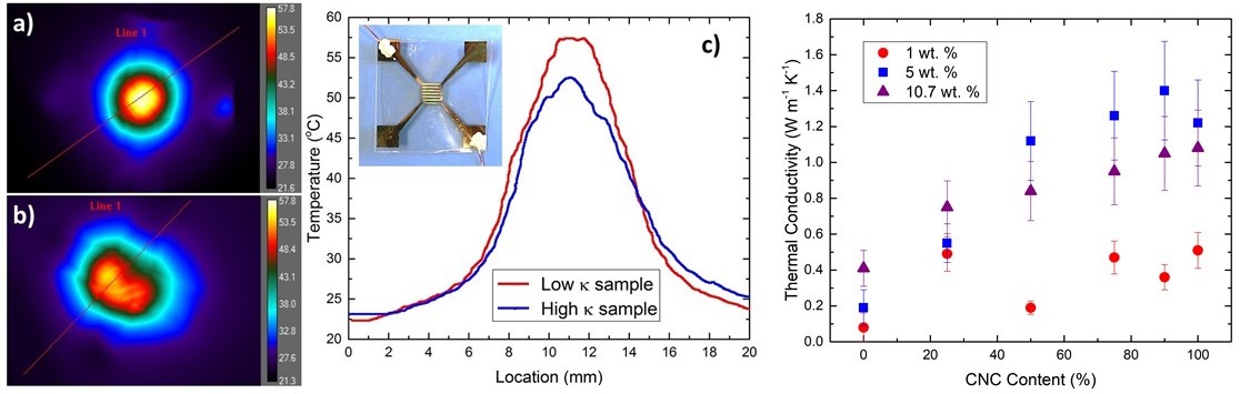
Superior, Processing-Dependent Thermal Conductivity of Cellulose Nanocrystal-Poly(vinyl alcohol) Composite Films (a) Thermal images of CNC-PVA composites a) 100 % PVA sample with low k , and b) 90:10 CNC:PVA sample with high k during Joule heating of a serpentine metallic heater simulating flexible electronics elements. c) Line scans along the centerline of a) and b) quantify the temperature reduction associated with the high k sample at the same Joule heating power (175 mW). Inset: Photograph of 90:10 CNC:PVA sample with shadow-evaporated metallic heater. (Right) Thermal conductivity of un-sheared CNC:PVA films versus CNC content of final film. Data shown is for 1, 5, and 10.7 initial CNC and PVA weight percent used during fabrication. The PVA molecular weight was 124-186K. Chowdhury, R. A., Rai, A., Glynn, E., Morgan, P., Moore, A. L., and Youngblood, J. P., “Superior, Processing-Dependent Thermal Conductivity of Cellulose Nanocrystal-Poly(vinyl alcohol) Composite Films,” Polymer 164, 2019, 17-25. DOI: 10.1016/j.polymer.2019.01.006 [Link]

A batch fabrication-compatible multifunctional thermal sensor based on thin film thermocouple and thermopile elements. (Top left) Annotated 3D model of the sensor design. Topmost oxide layer not shown. The sensor itself is 5 mm × 5 mm × 0.9 mm, while the thin film thermocouple/thermopilefeatures are 85–100 microns in width and 100 nm thick. Not to scale. (Top right) A close-up of the center of the wafer, a group of sensors still connected by scorelines, and an individual sensor that has been isolated from the parent wafer. (Bottom left) Light microscope images of the thermopile junctions at the edge of the main etch pit and at its center. (Bottom right) Voltage output from the thermopile element at 800 deg. C for increasing heat fluxsteps of 1.24 W cm−2, 2.28 W cm−2, and 4.96 W cm−2. Arrows indicate when system was at steady state at the corresponding heat flux. Khatri, N., Desai, T., Rai, A., KC, P., and Moore, A. L., "A Batch Fabrication-compatible Multifunctional Thermal Sensor Based on Thin Film Thermocouple and Thermopile Elements," Sensors and Actuators A 280, 2018, 188-196., DOI: 10.1016/j.sna.2018.07.038 [Link]

Flexible electronics-compatible non-enzymatic glucose sensing via transparent CuO nanowire networks on PET films TOP: FE-SEM images of CuO nanowires still adhered to the growth substrate. (a) CuO nanowires extending from surfaces of seed Cu microparticles deposited by electrodeposition. (b) Detail of one region shown in (a) in which sub-100 nm diameters and lengths on the order of microns are observed for all visible nanowires. (c) High magnification image of an individual nanowire with annotated diameter measurement. BOTTOM: (a) Top down photograph of an assembled sensor with color graphic behind it to demonstrate transparency. (b) Demonstration of device flexibility even with PDMS reservoir in place. (c) Annotated illustration of the glucose sensing experimental setup. The glucose solution under test is added to the internal volume bounded by the cylindrical PDMS reservoir’s walls. Bell, C., Nammari, A., Uttamchandani, P., Rai, A., Shah, P., and Moore, A. L., “Flexible Electronics-Compatible Non-enzymatic Glucose Sensing via Transparent CuO Nanowire Networks on PET Films,” Nanotechnology 28(24), 2017, 245502. DOI: 10.1088/1361-6528/aa7164 *Chosen for issue cover* [Link]
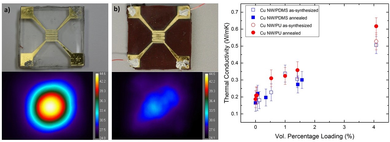
Thermal conductivity enhancement of PDMS and polyurethane via addition of copper (Cu) nanowires. a) A neat polyurethane sample with shadow-evaporated gold serpentine heater and its associated temperature map at steady-state after applying a fixed Joule heating power. b) An annealed Cu nanowire/polyurethane composite with 4.1 % volume copper nanowire loading and its associated steady-state temperature map after applying the same Joule heating power as was used for the neat polyurethane sample. c) Thermal conductivity of the tested materials at different volume percent loading of Cu nanowires. Rai, A. and Moore, A. L., “Enhanced Thermal Conduction and Influence of Interfacial Resistance within Flexible High Aspect Ratio Copper Nanowire/Polymer Composites,” Composites Science and Technology 144, 2017, pp. 70-78. DOI: 10.1016/j.compscitech.2017.03.020 [Link]
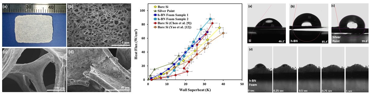
Pool boiling performance of foam-like h-BN as a surface enhancer. (Left) Images of foam-like h-BN nanomaterials: (a) freestanding foam with millimeter scale shown for reference, (b) FE-SEM large area view, (c) a single branched node, and (d) a fractured strut showing the hollow nature of the interior after selective etching of the parent nickel foam. (Middle) Boiling curves for vertically oriented bare silicon surface, silver painted surface, planar h-BN, and h-BN foam surfaces. Data for horizontally oriented bare silicon in DI water from literature are also plotted for comparison. (Right) Contact angle of water drop on (a) Si, (b) planar h-BN, and (c) silver paint surfaces. (d) Time-lapse images of h-BN foam showing its hydrophilic nature. KC, P., Nammari, A., Ashton, T. S., and Moore, A. L., "Saturated Pool Boiling Heat Transfer from Vertically Oriented Silicon Surfaces Modified with Foam-like Hexagonal Boron Nitride Nanomaterials," International Journal of Heat and Mass Transfer 95, 2016, pp. 964-971. DOI: 10.1016/j.ijheatmasstransfer.2016.01.006 [Link]
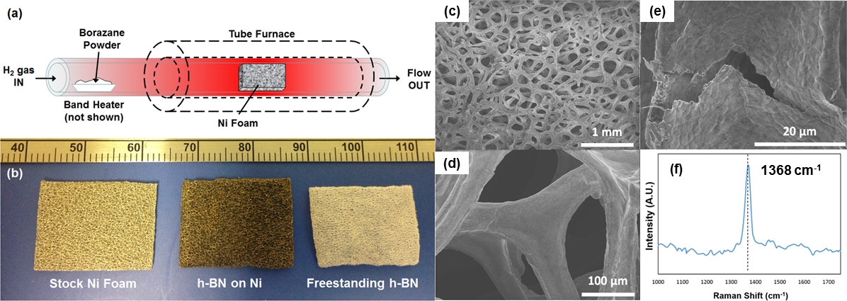
APCVD growth of foam-like hexagonal boron nitride (h-BN). (a) APCVD growth setup used by the PI’s group for creating hierarchical h-BN nanomaterials from Ni foam templates. (b) Scalable growth produces macroscopic freestanding samples once Ni has been selectively etched. (c-e) SEM image details (f) Raman spectrum revealing characteristic h-BN peak. Ashton, T. S., and Moore, A. L., “Three-dimensional Foam-like Hexagonal Boron Nitride Nanomaterials via Atmospheric Pressure Chemical Vapor Deposition,” Journal of Materials Science 50(18), 2015, pp. 6220-6226. DOI: 10.1007/s10853-015-9180-0 [Link]